|
|
|
|
|
|
|
|

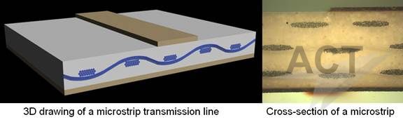
该用微带线还是带状线?这是高频设计师几十年来一直面临的抉择。这两种传输线技术均广泛应用于有源与无源微波电路中,效果良好。二者相比,是否其中一种更胜一筹呢?要解决此类问题,我们先来学习两种传输线的工作原理以及二者对印刷电路板(PCB)材料有何要求相关的内容,相信对该类问题的解决会有所助益。 微带线是传输线的一种,其特征是导体附着在一块下端面设有接地层的绝缘基材上。通常通过蚀刻去除导体层多余的金属而形成导体,例如铜。
带状线常被比作压平了的同轴电缆,这是因为它与电缆一样,由一个内导体构成,该内导体被绝缘材料完全覆盖,而绝缘材料又为接地编织线或金属箔所覆盖。当然,带状线电路在同一个平面上,因而呈现出“三明治”结构——中间为绝缘层所覆盖的导体,上部和下部面分别为互相平行的两个接地层。
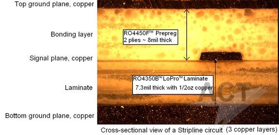
带状线电路的制造通常是采用粘合的方法,将顶层的绝缘基材及接地层或者用半固化片将带一层金属层的材料与已经蚀刻好线路的PCB层压板材料相粘结。若要避免带状线中产生多余的传播波形,必须缩短上下两个接地层之间的距离,这通常通过减小螺丝长度,或者采用PCB技术做金属化过孔的方式来实现。 为什么选择此传输线而非彼传输线呢?二者通过毫米波频率均可提供卓越的电气性能,这取决于PCB材料的选择。与带状线电路相比,微带线电路加工步骤少,且电路元件更易于放置,因而更易于制造(制造成本更低)。而比之微带线,带状线能够为相邻的电路线提供更多隔离,支持更密集的集成电路。此外,带状线电路还非常适合制造多层电路,各层能够良好隔离。层与层通过镀通孔(PTH)互连。 微带线与带状线导体的电气性能均受绝缘材料介电常数,以及接地层邻近效应的影响。微带线只有一个接地层,而带状线有两个接地层。对于微带线,影响导体阻抗的有效介电常数是绝缘材料及其电路上方空气的相对介电常数之和(等于1)。带状线的有效介电常数则为导体上下两个基材的相对介电常数之和。 对于所有高频电路,保持PCB的阻抗受控对于实现一致的振幅和相位响应电气性能至关重要。两种传输线的导体的阻抗除其它因素外,是导体宽度、导体厚度、绝缘基材的厚度,基材的相对电容率或介电常数的函数。对于带状线,中心导体与两接地层之间的距离是否相等,或者导体上下方绝缘体的介电常数是否相同并不重要(微带线亦是如此)。 带状线有两个接地层, 因此带状线的50Ω(或者任何给定阻抗)线比微带线阻抗相同的导体细。较细的线固然支持较大的电路密度,但是较细的线也需要更严格的制造公差,并且整个电路的基材的介电常数要非常一致。微带线的单端(不平衡式)传输线的介质损耗(由基材的耗散因子界定)比带状线少,这是因为微带线的一些场线在空气中,其耗散因子可忽略不计。 当然,这两种传输线所具备的性能实际上只是与其制造所用载体——绝缘基材的性能几乎相同。正如所采用的PCB材料,例如FR-4,能够降低成本,但同时也会限制其性能,根据不同的微带线和带状线应用选择最适宜材料,会更好地发挥这两种传输线的优点。 举例而言,介电常数低并且损耗低的PCB材料有益于微带线电路的设计,例如罗杰斯公司的RT/duroid® 5880。该材料基于损耗最低的聚四氟乙烯(PTFE)介质(频率为10 GHz条件下耗散因子仅为0.0004),为了比纯聚四氟乙烯有更高的机械稳定性,采用玻璃微纤维强化。其介电常数较低,并且严格控制,频率10 GHz条件下为2.20 ± 0.02,以便于保持微带线电路中导电线路的阻抗。当然,优异的性能必然不会便宜,并且材料的加工步骤需要严格控制,以实现整齐划一的产出。 微带线电路需要更低的介电常数,但是对介质损耗的要求不高,罗杰斯公司就此研发了RT/duroid 5880LZ 层压板,该材料由具有独特填充材料的聚四氟乙烯构成。频率为10 GHz 条件下,其介电常数为1.96 ± 0.04 ,典型耗散因子为0.0019。为了稳定,罗杰斯RO3003™介电材料采用陶瓷填料,并且对于微带线电路而言比价格相对较贵的RT/duroid 5880材料更易于制造。代价是其介电常数较高,在频率为10 GHz 条件下3.00±0.04,并且介质损耗增加,在频率为10 GHz 条件下0.0013 ,但是在频率为30GHz~40 GHz条件下仍然可用。 带状线电路具有“分层”性质,因而特殊应用通常选用“一套”介质材料而非某一种材料,例如结合使用罗杰斯公司的RO4350B™层压板及RO4450F™半固化片。电路蚀刻在RO4350B 材料上,两面均有金属。RO4450F半固化片用作粘结层,构成上绝缘层与上接地层的是只有一面带金属的基材。在成本和易于加工方面,RO4350B材料与FR-4材料相似,但是与上文所述的微带线电路材料相比,介电常数相对较高,在频率为10 GHz 条件下3.48 ±0.05,介质损耗也相对较高,在频率为10 GHz 条件下0.0037。 RO4350B层压板是玻璃纤维布强化的碳氢化合物和陶瓷材料(非聚四氟乙烯),尺寸稳定性良好。其搭档RO4450F半固化片在频率为10 GHz 条件,介电常数为3.52±0.05,耗散因子为0.004,两个参数均与RO4350B 层压板的参数极为匹配。带状线电路通常使用2 片或2 片以上的半固化片,对于要求电路层之间隔离度较高的应用尤其如此。如上文所述,带状线各层的介电常数和厚度可以不同,但在设计审查流程中应当对这些因素作出说明。 与许多工程决策一样,会权衡考虑选择微带线还是带状线。例如,带状线电路的电路密度高,因而,在相同频率条件下,比微带线电路需要更多的材料层、更多加工时间和费用、并且更需要注意细节的处理。不管怎样,不论是基于微带线技术还是带状线技术,各种PCB材料都能够帮助设计师针对特定设计实现最佳性能。
Microstrip or stripline? That choice has been faced by high frequency designers for decades. Both transmission-line technologies are widely used in both active and passive microwave circuits, with excellent results. Is one approach better than the other? Before tackling such a question, it might help to know how each transmission-line technology works and what kind of demands each place on a printed circuit board (PCB) material. Microstrip is a transmission-line format in which the conductor is fabricated on a dielectric substrate which itself has a bottom ground-plane layer. Conductors are usually formed by etching away unwanted metal from a conductor layer, such as copper. Stripline is often compared to a flattened coaxial cable in that, like the cable, it consists of an inner conductor completely surrounded by dielectric material which is itself surrounded by a ground braid or foil. Of course, stripline circuits are planar, so that they appear as a sandwich of conductors in the middle, surrounded by dielectric layers, which in turn have parallel ground planes on the top and bottom. Stripline circuits are usually fabricated by adhesively bonding a top-layer dielectric substrate/ground plane or prepreg with a single metal layer to a PCB laminate material on which circuitry has been photo-etched. To avoid unwanted propagation modes in stripline, the two ground planes must be shorted, often by means of shorting screws, or in the case of PCB technology, plated through hole via’s. Why choose one transmission-line format over the other? Both provide excellent electrical performance through millimeter-wave frequencies, depending upon the choice of PCB materials. Microstrip circuits are easier (and less expensive) to fabricate than stripline, with less processing steps and easier placement of circuit components. The stripline format affords more isolation between adjacent circuit traces, supporting more densely integrated circuits than with microstrip. Stripline circuits are also well suited for fabricating multilayer circuits, with good isolation between layers. The layers are interconnected by means of plated through holes (PTHs). In both microstrip and stripline, the electrical behavior of the conductors are affected by the relative dielectric constants of the insulator materials as well as the proximity of the ground planes. In microstrip there is one ground plane, while in stripline, there are two. In microstrip the effective dielectric constant impacting the impedance of a conductor is a combination of the relative dielectric constant of the insulator material as well as that of the air above the circuit (which is equal to 1). In stripline the effective dielectric constant is a combination of the relative dielectric constants of the substrate layers above and below the conductors. For any high frequency circuit, maintaining controlled impedance across a PCB panel is critical to achieving consistent electrical performance in terms of amplitude and phase responses. The impedance of a conductor in either transmission-line format is a function of the width of the conductor, the thickness of the conductor, the thickness of the dielectric substrate, and the relative permittivity or dielectric constant of the substrate, among other things. In stripline it is not critical that a center conductor be equally spaced between the two ground planes, or that the insulators above and below the conductor have the same dielectric constant (as is the case with microstrip). Because of the second ground plane, the width of a 50-Ω (or any given impedance) line in stripline will be narrower than for a conductor with the same impedance in microstrip. While the inherently thinner lines support greater circuit densities, they also require tighter fabrication tolerances as well as substrate materials with extremely consistent dielectric constant across a board. For a single-ended (unbalanced) transmission line in microstrip, dielectric losses (defined by a substrate’s dissipation factor) will be less than for stripline, since some of the field lines in microstrip are in air where the dissipation factor is negligible. Of course, the performance available from either of these transmission-line formats is only as good as the performance of the dielectric substrates upon which they are fabricated. Just as the use of a PCB material such as FR-4 will cut costs but limit performance, choosing materials optimized for different microstrip and stripline applications can better take advantage of the benefits of each transmission-line format. For example, microstrip circuit designs can benefit from a PCB material with a combination of low dielectric constant and low loss, such as RT/duroid® 5880 from Rogers Corporation. It is based on polytetrafluoroethylene (PTFE) dielectric for minimal loss (a dissipation factor of only 0.0004 at 10 GHz), but reinforced with glass microfibers for enhanced mechanical stability compared to pure PTFE. The dielectric constant is low and tightly controlled, 2.20 ± 0.02 at 10 GHz, in order to maintain the impedance of conductive traces fabricated in microstrip circuits. Of course, premium performance is not inexpensive, and the material requires tightly controlled processing steps to achieve consistent yields. For microstrip circuits requiring an even lower dielectric constant, but where dielectric loss is less critical, Rogers developed RT/duroid 5880LZ laminate, consisting of PTFE with a unique filler material. It exhibits a dielectric constant of 1.96 ± 0.04 at 10 GHz with typical dissipation factor of 0.0019 at 10 GHz. Rogers RO3003™ dielectric materials use ceramic loading for stability, and are easier to fabricate for microstrip circuits than more costly RT/duroid 5880 materials. The tradeoff is in higher dielectric constant, 3.00±0.04 at 10 GHz, and increased dielectric loss, 0.0013 at 10 GHz, although they are nonetheless usable at frequencies through 30 to 40 GHz. With the “layered” nature of stripline circuits, a dielectric “system” rather than a single material is usually selected for a particular application, such as the combination of RO4350B™ laminate and RO4450F™ prepreg from Rogers. Circuits are etched on the RO4350B dielectric material, which is metalized on both sides. The RO4450F prepreg is used as a bonding layer, which is metalized on only one side, forming the top dielectric layer and top ground plane. The RO4350B material is similar to FR-4 materials in terms of cost and ease of processing, although with higher dielectric constant, 3.48 ±0.05 at 10 GHz, and dielectric loss, 0.0037 at 10 GHz, than the materials mentioned above for microstrip circuits. Fabricated from glass-reinforced hydrocarbon and ceramic laminate materials (not PTFE), RO4350B laminate provides excellent dimensional stability. Its companion, RO4450F prepreg material, has a dielectric constant of 3.52±0.05 at 10 GHz and dissipation factor 0.004 at 10 GHz, both parameters closely matched to those of RO4350B laminate. Two or more plies of prepreg are typically used in stripline circuits, especially in applications requiring high isolation between circuit layers. As mentioned earlier, the dielectric constants and thicknesses of stripline layers can differ, although these factors should be accounted for during any design review process. As with many engineering decisions, a choice between microstrip and stripline involves considering a number of tradeoffs. The high circuit density of stripline, for example, requires more material layers, processing time and expense, and attention to detail than for microstrip circuits operating at the same frequencies. In either case, a variety of PCB materials are available to help a designer achieve the best performance for a given design, whether it is based on microstrip or stripline technology.
版权声明: 《华体会体育推荐 》网站的一切内容及解释权皆归《华体会体育推荐 》杂志社版权所有, 未经书面同意不得转载,违者必究! 《华体会体育推荐 》杂志社。 |
|
|||||||||
 |
友情链接 |
| 首页 | 关于我们 | 联络我们 | 加入我们 | 服务条款 | 隐私声明 Copyright© 2025: ; All Rights Reserved. |
 |
 |